PCB Panel Layout: Maximize Efficiency in Your Designs Pcb layout
If you are looking for Altium designer pcb panelization - lockqsmart you've came to the right place. We have 25 Pics about Altium designer pcb panelization - lockqsmart like KiCad PCB Panelization with Javascript | Climbers.net, How to Design a PCB Layout - Circuit Basics and also Altium designer pcb panelization - lockqsmart. Read more:
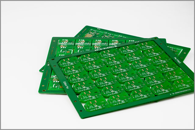
Altium Designer Pcb Panelization - Lockqsmart
 lockqsmart.weebly.com
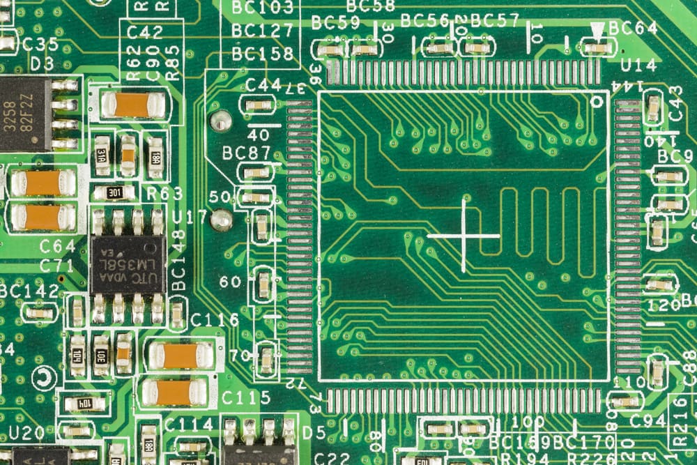
How To Design A PCB Layout - Circuit Basics
 www.circuitbasics.com
pcb layout circuits electronics campbell posted
PCB Panel Sizes | Standard PCB Dimensions, Board Sizes
 www.ourpcb.com
pcb circuit layers enig proto prototype pcbs fabrication hasl wellpcb ourpcb breadboard plating depends separate
Amplifier PCB Layout: Designing For Efficiency And Performance
 jamindopcba.com
The Surprising Secret To Designing Combination Method Of PCB Panels
 www.pcbcart.com
pcb method combination panel panelization designing panels surprising secret
(PDF) PCB Layout Tips To Maximize ESD Protection Efficiency - … · 2021
 pdfslide.net
How Do You Make A PCB Panel ? - RayMing PCB
 www.raypcb.com
pcb panel panelization different two production figure designs manufacturing board design testing make do assembly same
Optimizing PCB Layout For Assembly And Manufacturing Efficiency
 microcad3d.com
What Is A PCB Panel? PCB Panelization Guide. - JHDPCB
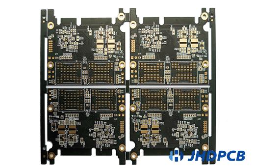 www.jhdpcb.com
What Is PCB Panelization?
 www.jycircuitboard.com
pcb panelization small what include manufacturing however batch grouping limitations limited following its also use some
Enhanced PCB Design Efficiency With Mouse Bites
Get 33% Better Efficiency On Your PCB Panels. - YouTube
 www.youtube.com
pcb
PCB Layout: Selecting The Track Width And Spacing For A Differential Signal
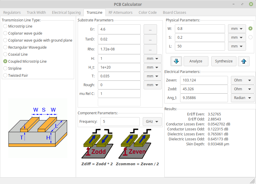 billauer.co.il
pcb spacing layout differential microstrip selecting
Thermally Optimizing A High-Power PCB For Battery Powered Electronics
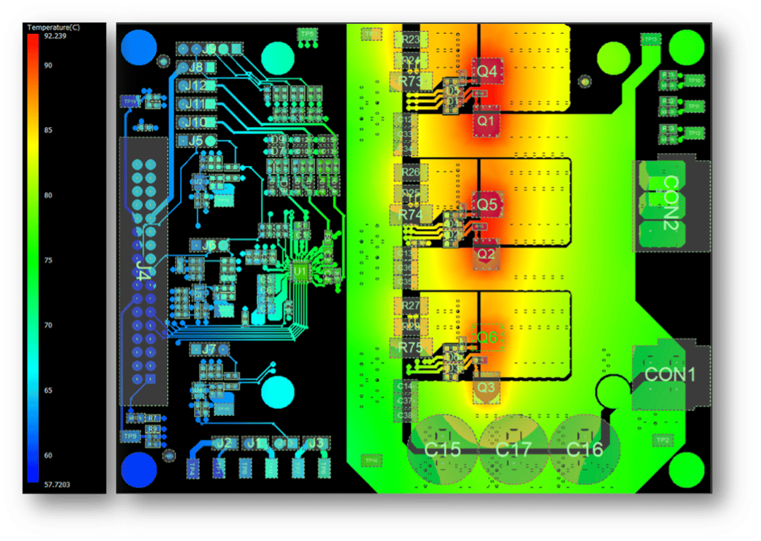 www.electronics-cooling.com
Physical Design Reuse In PADS: How To Leverage Corporate IP To Increase
 www.pads.com
pads design pcb physical efficiency reuse increase leverage corporate ip
PCB Panel Design Rules For Efficient Laser Depaneling
 laser-depaneling.lpkf.com
pcb depaneling panel lpkf gpus
What Is PCB Panelization?
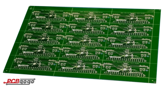 www.pcbgogo.com
panelization pcb pcbs
Expert PCB Routing: 31 Tips To Maximize Efficiency & Reliability
 www.rowsum.com
PCB (Printed Circuit Board) Panel Design Consideration
 www.optimatech.net
pcb panel design board circuit printed consideration what
8 Rules And Methods Of PCB Panel – PCB HERO
 www.pcb-hero.com
KiCad PCB Panelization With Javascript | Climbers.net
 climbers.net
pcb panelization panel kicad javascript jlcpcb climbers panels why pcbs
The Ultimate Guide To Optimizing Your PCB Layout For Efficiency - Top
 camtechpcb.com
PCB Layout - Mentor Graphics
 www.mentor.com
pcb layout sketch mentor routing xpedition assisted interactive technology auto
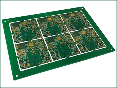
What Is PCB Panelization & Why Do We Need It? - The Engineering Projects
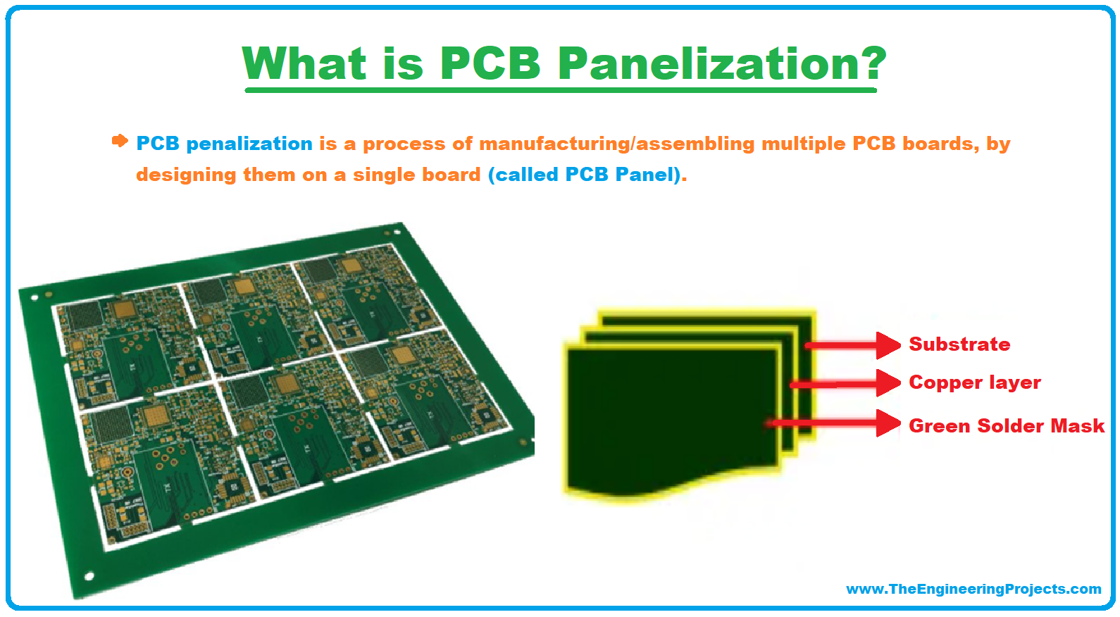 www.theengineeringprojects.com
How To Design A PCB Layout: A Comprehensive Guide
 www.wevolver.com
Pcb circuit layers enig proto prototype pcbs fabrication hasl wellpcb ourpcb breadboard plating depends separate. How do you make a pcb panel ?. (pdf) pcb layout tips to maximize esd protection efficiency